CMOS Annealing Transition
"Relaxed MA" that supports continuous variables such as minority.
June 2024
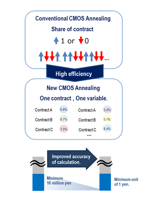
By developing an algorithm to solve optimization problems that include both discrete and continuous variables, we have significantly expanded the number of digits that can be computed.
In the past, CMOS annealing has been specialized in binary variable optimization problems. However, with this development, calculations including continuous values such as decimals have become possible, significantly improving the accuracy of optimization calculations.
By applying it to insurance portfolio optimization, it is now possible to calculate in units of 1 yen, which was previously only possible in units of at least 10 million yen. It also allows for considering a large number of combinations in a single calculation.
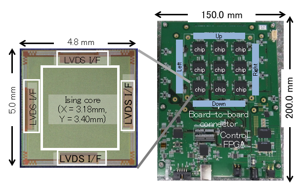
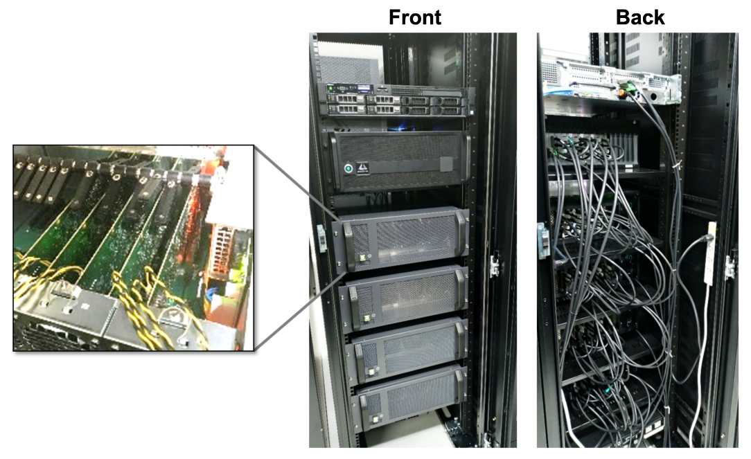
We demonstrated operation with 3x3x9 boards = 81 chips connected (1.3M spins)
November 2021
We demonstrated the cooperative operation of 81 chips by vertically and horizontally connecting the 9-chip connection board which was announced in February 2021.
We have shown that it could grow indefinitely as long as the boards are connected. We will be able to meet customers’ demand for larger scale.
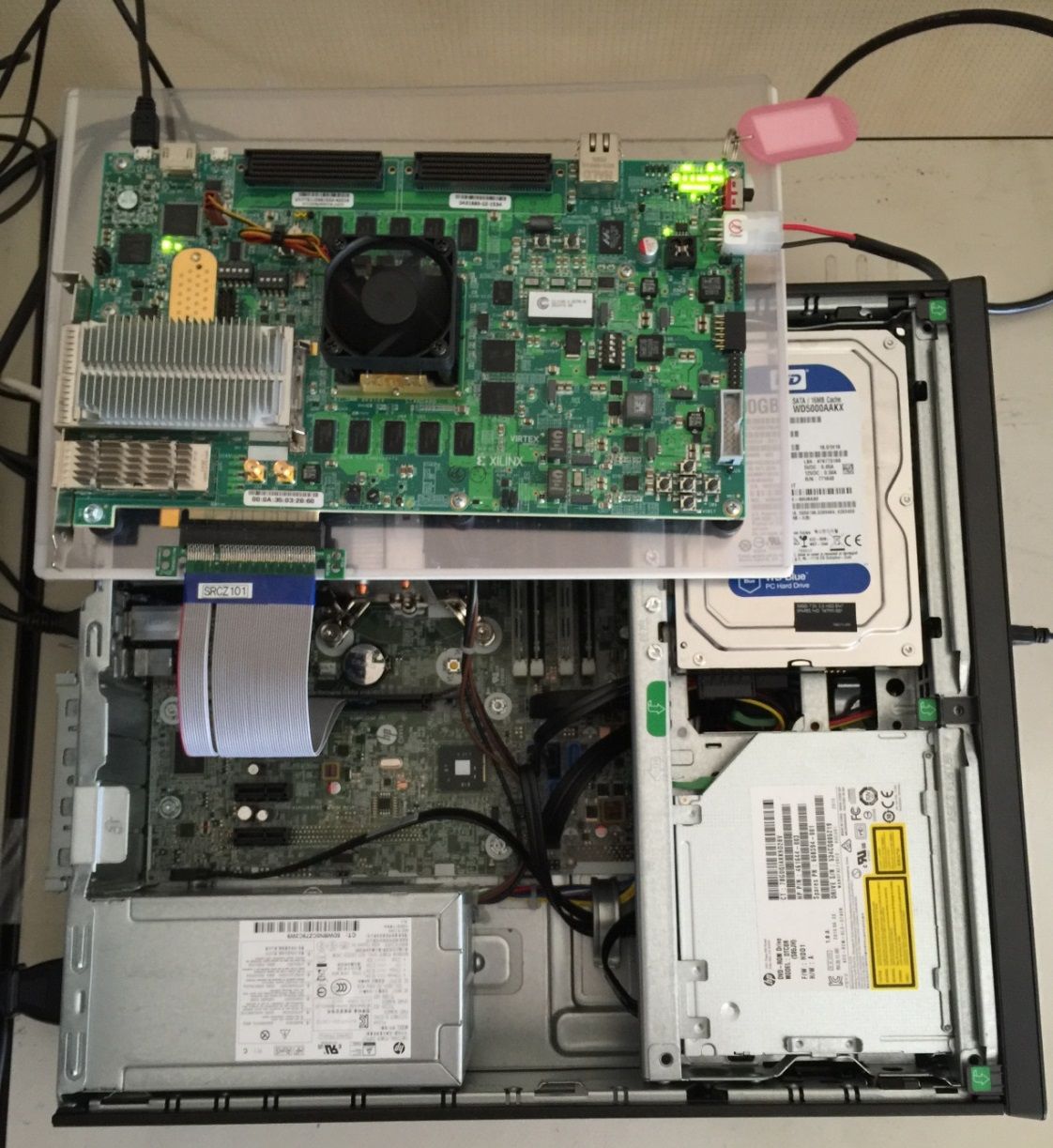
We demonstrated 3x3 = 9 chip connection operation (144k spins)
February 2021
Even Bigger: The Birth of a CMOS Annealing Machine with 9 Chips Connected in 3 directions
Two years after the announcement of the business-card-sized prototype, as a result of the NEDO project, we announced a new CMOS annealing machine that can handle 144k spins by connecting 9 CMOS annealing chips vertically, horizontally, and diagonally. It shows that it can be infinitely enlarged in two dimensions by connecting them. The machine can be connected to an infinite number of chips in two dimensions, hoping to meet the demand for even larger scales in the future.
This is the ASIC version of the annealing machine implemented and serviced by this cloud service.
We implemented GPU for Annealing Cloud Web (King's graph version)
August 2020
We began to provide a software version of the annealing machine which can run on our API to accelerate App search.
We have implemented an environment to run the annealing of an ASIC version of the CMOS annealing machine as software on a GPU, supporting 256k spins and having a 32-bit coefficient width. It supports 256k spins and has a 32-bit coefficient width. We aim to accelerate the exploration of applications by testing problems that cannot be solved in hardware.
This is the GPU (King's graph) version of the annealing machine implemented and serviced by this cloud service.
We announced Momentum Annealing Edition
August 2019
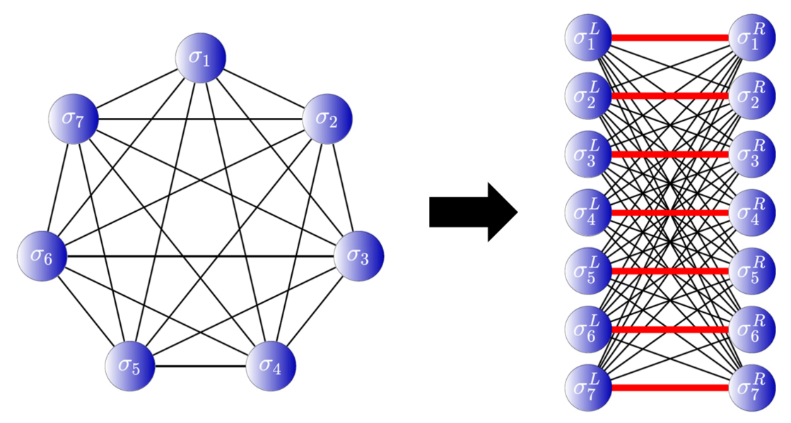
We announced full-coupled CMOS annealing. That is the Momentum Annealing (MA) version.
We presented an algorithm for ground-state search of the all-coupled Ising model. We implemented it on a GPU and proved to be 250 times faster than the conventional optimized SA method.
More...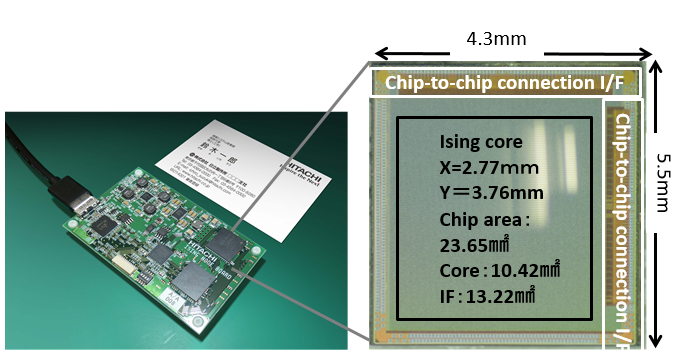
We announced a business card-sized CMOS annealing machine (60k spins)
February 2019
We developed a two-chip business-card size CMOS annealing machine as a result of the NEDO project.
In a NEDO project started in 2016, Hitachi had been working on developing a large-scale CMOS annealing machine, and created a prototype that operates by connecting two chips together. The result turned out to be the world's smallest hardware. It ended up being just as small as a business card, but the annealing machine can handle 30,976 x 2 = 61,952 spins, consumes less energy, and operates over a USB connection. We have also shown that it can be embedded in edge devices.
Annealing Cloud Web was open
August 2018
We demonstrated a large scale CMOS annealing machine with 25 FPGAs connected (100k spins)
June 2018
We were able to successfully connect 25 FPGAs to run as one giant CMOS annealing machine.
In 2018, we successfully connected 25 FPGAs to operate as a single CMOS annealing machine. This enabled the hardware to handle a large scale combinatorial optimization problem with 102,400 spins. Expanding on this achievement, later ASIC prototypes were extended by connecting the chips. We have shown that scalable computation can be achieved by computing digitally.
We made a prototype FPGA version of CMOS annealing machine and improved the accuracy of the solution.
November 2016
We made the second generation of FPGA prototypes for implementation and app search.
We implemented the second-generation prototype which was released in 2016 in an FPGA. By sharing the processing of parameters among multiple elements, we were able to reduce the circuitry to 1/10 size of the previous prototype in the same machine area, while also improving the computational accuracy. The programmable prototype has further accelerated the research and development of subsequent CMOS annealing machines.
NEDO IoT cross-sectional project started
August 2016
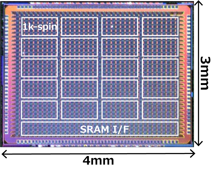
We announced the first CMOS annealing chip (20k spins)
February 2015
We presented the first CMOS annealing chip at the ISSCC2015 event.
We presented a CMOS annealing machine that is the world's first ising machine implemented in semiconductor CMOS and operating at room temperature.